
Head:
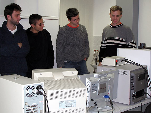
Ing. Daniel Haško, PhD.,
Scope of the Laboratory:
Application and development of scanning microscopic techniques for structural and surface diagnostics of materials, micro- and nano-structures applicable in progressive electronic and optoelectronic devices.
Research activities:
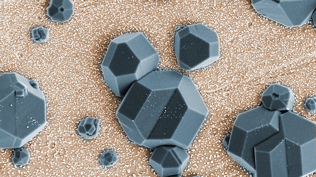
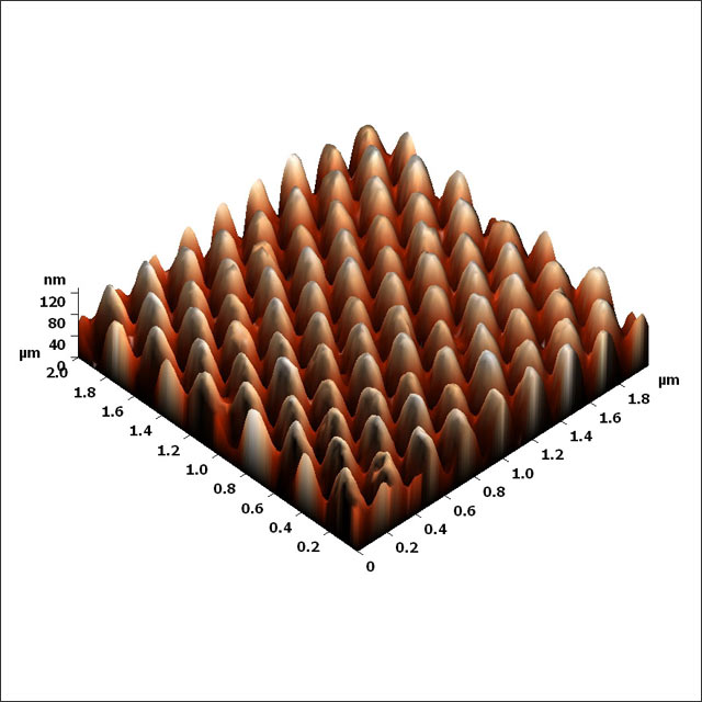
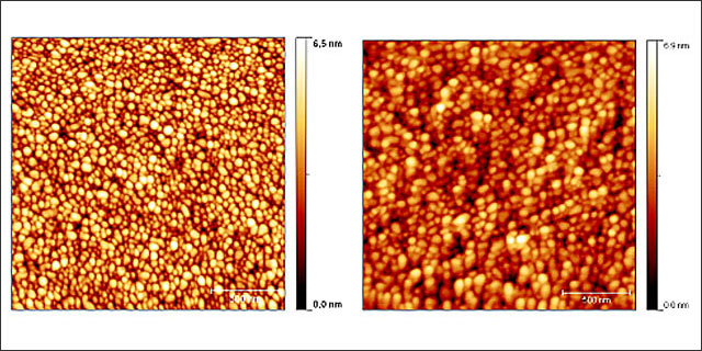
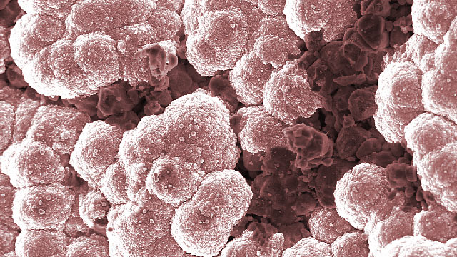
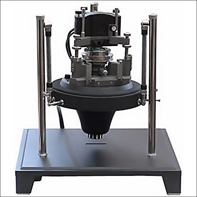
Our activities are oriented on characterization of structural properties of materials and surfaces of various objects using field emission scanning electron microscopy (FE SEM), atomic force microscopy (AFM) and scanning tunnelling microscopy (STM). FE SEM with spatial resolution up to 1 nm utilized for surface morphology visualization of semiconductor structures and devices oriented to nano-scaled layers, nanoparticles and its element analysis. AFM and STM techniques are used for surface imaging, complementary structural and surface roughness analysis with high resolution down to atomic scale as well as measurement of local physical properties such as geometrical relief, surface conductivity, distribution of electric potentials, electrostatic and magnetic forces on the surface layer.
Selected Applications:
- nanometrology of nanostructures and nanostructured surfaces,
- inorganic and organic semiconductor materials, layers and nanoparticles (Si, GaAs, InP, GaN, ZnO, SiC, pentacene, parylene, rubrene, parasexyphenyl …),
- electronic structures and devices,
- magnetic nanoparticles, nanorods and nanomaterials,
- carbon nanotubes and nanoobjects, diamond and diamond-like carbon layers,
- nanostructured surfaces prepared by nanoreplication techniques,
- photonic structures and devices,
- biologic nanomaterials and objects

|
|
|
|
|